ECO-3451 · REV J · effective November 17, 2026
EV Manufacturing TransitionRELEASEDEngineering notice
Infineon processes SiC on 300 mm wafers for first time in Villach
Infineon ran 300 mm silicon carbide wafers in production conditions at Villach, claiming an industry first. Each wafer yields 2.3x the chips of 200 mm, but no ramp timeline has been set.
Scope of change
- Infineon processed 300 mm SiC wafers under production conditions for the first time at Villach, Austria.
- A 300 mm wafer yields approximately 2.3 times as many chips as a 200 mm wafer, per Infineon.
- No timeline for the 300 mm SiC production ramp has been set; it will be decided with customers and partners.
- Infineon plans around €1.1 billion of investment in Villach by 2034; GaN high-volume 300 mm output starts end of 2027.
- Cold-split technology for 300 mm SiC was successfully tested in Dresden, reducing material loss versus wire sawing.
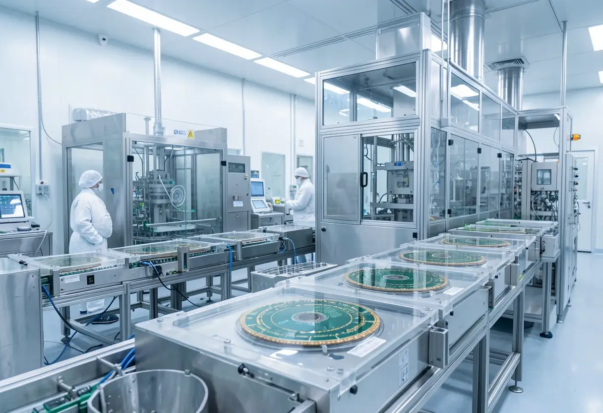
Infineon has processed 300 mm silicon carbide wafers under real production conditions for the first time, running the material at its plant in Villach, Austria. The company says it's the first semiconductor manufacturer to reach this milestone, and it did so in existing cleanroom facilities that also handle silicon.
The number that matters: a 300 mm wafer carries roughly 2.3 times as many chips as a 200 mm wafer, according to Infineon. That's the whole economics of the move. More die per wafer means better scaling of SiC output as demand from EV makers climbs.
What's missing is a timeline. Infineon has not set a date for ramping 300 mm SiC production, saying it will determine timing together with customers and partners. The existing 200 mm SiC roadmap continues unchanged in parallel. So treat this as a proven process capability, not a confirmed capacity plan.
Why SiC matters for automotive
Silicon carbide is a wide-bandgap material (a semiconductor class that handles higher voltages and temperatures than standard silicon). Compared with silicon, SiC delivers lower power losses and higher power density. On the vehicle side that shows up in traction inverters (the unit converting battery DC to motor AC), on-board chargers, and DC fast-charging stations, plus stationary storage and industrial drives.
For e-mobility buyers, the 300 mm step is about scale and manufacturing cost. More chips per production run could make high-volume SiC output cheaper over the long term. Infineon has made no claims about cost reductions per component, though. That question stays open until a ramp is dated and volumes land.
Cold-split tested in Dresden
Infineon is also attacking the wafer-making side of the equation. At its Dresden site, the company has successfully tested cold-split technology on 300 mm SiC. The method separates wafers from a SiC crystal with less material loss and shorter processing time than conventional wire sawing, so more wafers come out of each crystal. Material yield at the crystal stage is a major cost driver in SiC, so this matters as much as the fab-side milestone.
The 300 mm strategy behind it
The SiC demonstration builds directly on Infineon's existing 300 mm push in Villach. The company had already prepared the shift from 200 to 300 mm for gallium nitride, and at the end of October it announced roughly €1.1 billion of investment at the site through 2034. High-volume GaN power semiconductor production on 300 mm wafers is scheduled to start at the end of 2027.
With SiC now on the same platform, Infineon produces power semiconductors on silicon, gallium nitride, and silicon carbide, and relies on 300 mm technology across all three materials. That commonality is the strategic point: one fab approach, three material systems.
What to watch next: a dated 300 mm SiC ramp plan from Infineon, customer commitments that anchor those volumes, and whether the cold-split process moves from successful test to series wafer production in Dresden.
via electrive (Source)
More from Grace Kim
Show full bio
Staff writer covering people, launches and day-to-day practice in Automotive manufacturing and vehicle production at Autoplant Brief.
293 articles
Also circulated
- Infineon to Pour €1.1 Billion into Villach GaN Chip Plant by 2034
- India Targeting 50 Million Vehicle Output by 2030
- GlobalFoundries to spend $21 billion on New York fabs under US-Japan deal
- Automotive Metalworking Outlook Runs to 2035 on EV Demand
- Bosch splits semiconductors into standalone division from 2028